Calidad
Enemies of photovoltaics - LID effect
We continue to expand our series of articles on quality, enemies of photovoltaics. This time we want to talk about a phenomenon known and studied since the 70s, the LID (Light Induced Degradation) effect. This consists of a degradation of the photovoltaic modules due to chemical reactions in the silicon cell caused by the presence of impurities found in the materials used and their processing method during manufacturing.

What is LID?
This phenomenon consists of a loss of power and therefore efficiency, which occurs in silicon modules. The loss is created during the first months of exposure to solar irradiation and, to date, a way to completely prevent its appearance has not been discovered. This degradation can lead to losses of up to 10% of the initial power.
Why does it occur?
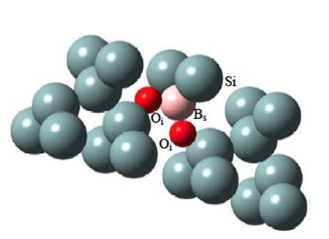
It is mainly produced by the reaction of boron with other chemical elements present in the cell, such as oxygen, iron or copper.
We might think that eliminating or decreasing the boron in the cells would solve the problem, but this would lead to a reduction in module efficiency. Therefore, when manufacturing the photovoltaic cell, the amount of boron must be optimally balanced, as it is an essential silicon dopant for electricity generation. The action of "doping a cell" with boron consists of enriching the silicon with this element, which gives it the capacity to transport electrons.
If we focus on how oxygen affects it, for example, we observe that it reacts forming a stable structure that we call "boron-oxygen complex". When this bonding occurs, the boron loses the space necessary to allow the flow of electrons within the cell (called the "gap"), resulting in a decrease in performance.
Therefore, the incidence of this effect will be determined by the quality of the raw material in the silicon wafer.
You can see the molecular structure of the Oxygen and Boron present in the silicon cell.
Although great progress has been made in this regard, the LID effect remains a priority to be addressed in module development. The PV industry continues to investigate this phenomenon and to make great efforts to eliminate or limit the defects caused by LID.
How is LID detected?
t is not a problem that we can detect with the naked eye. The first symptom of the LID phenomenon, to which we should pay attention, is a drop in panel performance. If any change in production is detected, we would have to use specialized electroluminescence equipment to measure the damage.
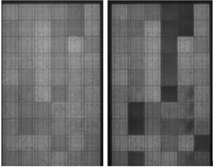
Electroluminescence is an "X-ray of the module" that allows us to see defects that escape visual inspection. During this process, the maximum current (Isc) is injected into the module, causing it to emit radiation at a frequency only visible with special filters and cameras. In the measurements we take, we will be able to see white, gray and black areas indicating the damage it has suffered. Areas with darker colors will be the ones with no electrical activity and therefore the ones that will decrease the panel's performance.
This is an example of how a module is affected by LID: initial (left) and after exposure to irradiation (right).
How do you avoid the effects of LID?
After years of development and research to prevent the occurrence of this phenomenon, some manufacturers have succeeded in reducing LID losses to less than 2%. This is done through techniques such as:
- Applying high temperatures.
- Injecting high currents.
- Applying advanced laser or LED technologies.
Another technique that obtains great results is the elimination of oxygen inside the cell. The disadvantage is that currently the technology needed to do this is very expensive, which translates into uncompetitive prices. Some manufacturers have adopted the solution of replacing boron with gallium.
Does it occur equally in all modules?
Although this effect is something that happens in all modules, it particularly affects "p-type" monocrystalline modules. This is because oxygen cannot be completely removed during the manufacturing process.
One measure that almost completely avoids the occurrence of LID is the use of n-type cells. The architecture of these cells prevents the combination of boron and oxygen in the bulk layer of the cell.
Here we can see what the PERC n-type and p-type cell structure looks like.
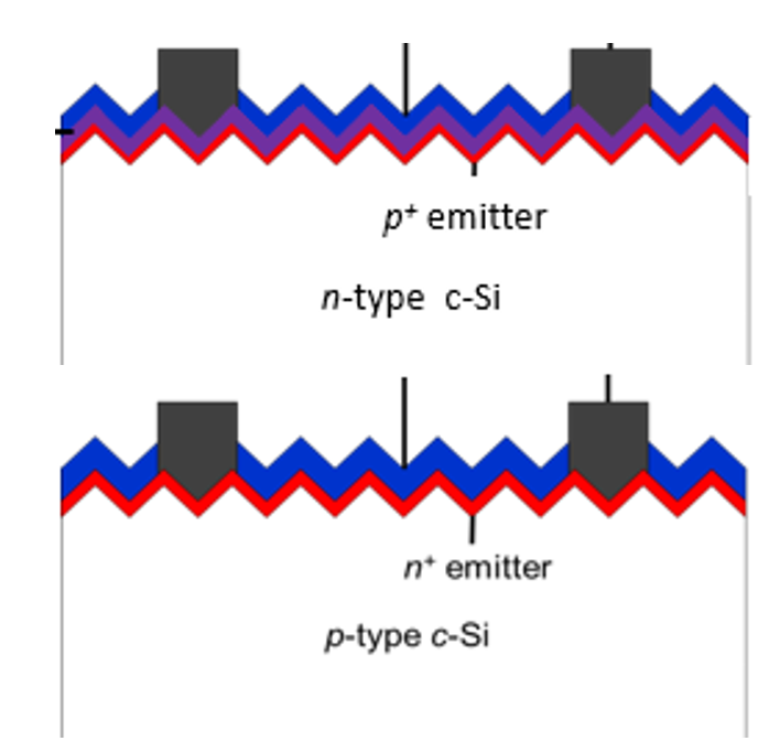
This occurs because n-type cells are manufactured virtually “in reverse” of the p-type cell. The large central layer is not doped with boron, but with phosphorus. As there is no boron in the bulk layer of the cell, boron-oxygen complexes cannot form.
Conclusion
To avoid the LID effect, it is important to carefully choose the materials and therefore the manufacturers of the materials, since a large part of the responsibility lies with them. Wafer treatments should be optimized to reduce the phenomenon, including further steps if necessary during the production chain to improve the strength of the material.
It is essential to take all these variables into account, since the life of our installation and its performance over time will depend on them. We will also be able to avoid or mitigate the appearance of the "enemies of photovoltaics".